
www.medical-devices.tech
14
'26
Written on Modified on
Siemens Healthineers Opens Europe’s First Photon-Counting Sensor Fab
€100 million facility manufactures CdTe semiconductor sensors for photon-counting CT scanners, supporting sharper imaging, reduced radiation exposure and expanded European production.
www.siemens-healthineers.com
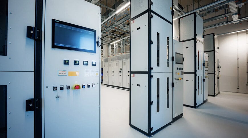
Siemens Healthineers has inaugurated a semiconductor manufacturing plant at its Forchheim, Germany facility, dedicated to producing cadmium-telluride semiconductor sensors for photon-counting computed tomography scanners. The facility represents an investment of approximately 100 million euros, covering 9,500 square meters of floor space to handle industrial-scale synthesis, crystal growth, and lithographic sensor processing for medical diagnostic systems.
Solid-State Crystal Synthesis and Cleanroom Fabrication
Photon-counting computed tomography replaces standard energy-integrating scintillators with direct-converting semiconductor materials. Conventional CT detectors rely on a two-step conversion process: incoming X-ray photons strike a scintillator material to generate visible light, which is subsequently converted into electrical signals by a photodiode. Direct-conversion semiconductor sensors absorb X-ray photons directly, instantly generating electron-hole pairs and voltage pulses proportional to the energy level of each individual photon. This direct measurement eliminates optical crosstalk, enhances spatial resolution, and reduces radiation dose requirements.
The Forchheim facility integrates the complete manufacturing workflow for cadmium telluride sensors. Synthesizing these compounds requires bonding ultra-pure cadmium and tellurium at temperatures of approximately 1,100 degrees Celsius. The crystal growth cycle spans approximately ten weeks to produce uniform single-crystal ingots.
Following growth, ingots undergo precision cutting and surface polishing to submillimeter tolerances. In cleanroom environments, photolithography processes define pixel matrices on the polished substrates, transforming bulk crystals into detector arrays ready for integration into clinical imaging gantries.
Production Scalability and Infrastructure Design
The European plant provides dual-source supply redundancy alongside the company's existing semiconductor facility in Japan, which operates near maximum capacity limits. To support industrial processing of high-purity heavy metals, the facility incorporates dedicated air emission filtration and multi-stage wastewater treatment units, representing a single-digit million-euro capital allocation within the broader facility development.
The infrastructure holds LEED Platinum certification and operates with net-zero operational carbon emissions. Process waste heat supplies building climate control loops, supplemented by a 170 kWp rooftop photovoltaic array. Building surroundings incorporate light-reflective paving and native flora to reduce urban heat island effects and maintain local biodiversity.
According to Uwe Rückl, Head of CT Detectors and Crystals at Siemens Healthineers, centralizing single-crystal growth and wafer-level fabrication in Forchheim aligns detector production directly with local computed tomography engineering lines, supporting increasing clinical deployment rates.
Additional Context:
This section details technical specifications and competitive benchmarking not included in the original product announcement
Direct-conversion photon-counting detectors are benchmarked by energy resolution, spatial resolution, charge collection efficiency, and count-rate capability measured in millions of counts per second per square millimeter before pulse pile-up occurs.
Siemens Healthineers remains the primary commercial manufacturer utilizing cadmium telluride crystals in clinical whole-body systems, exemplified by the Naetom Alpha platform. Cadmium telluride provides high stopping power for diagnostic X-ray spectra between 20 and 140 keV due to high atomic numbers (cadmium Z=48, tellurium Z=52) and a density of 5.85 g/cm³. However, cadmium telluride crystals are historically susceptible to polarization phenomena and hole-trapping under intense diagnostic X-ray flux, necessitating specialized crystal doping and high-voltage bias management.
Competing system manufacturers pursue alternative direct-conversion materials. GE HealthCare evaluates deep-silicon detector architectures through its Prismatic Sensors subsidiary. Silicon offers high carrier mobility, absence of polarization drift, and compatibility with established commercial semiconductor foundries. However, silicon possesses a lower atomic number (Z=14) and density (2.33 g/cm³), requiring edge-on orientation and long physical absorption depths to capture high-energy diagnostic photons efficiently. Meanwhile, Philips and Canon Medical Systems benchmark cadmium zinc telluride (CdZnTe) substrates, which offer wider bandgaps and lower leakage currents than pure cadmium telluride at ambient temperatures, though large-area industrial crystal growth yields remain a primary manufacturing challenge across the industry.
Edited by Natania Lyngdoh, Induportals editor, assisted by AI.
www.siemens-healthineers.com

